Double-Sided PCB
Description:
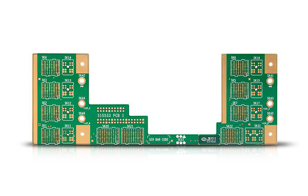
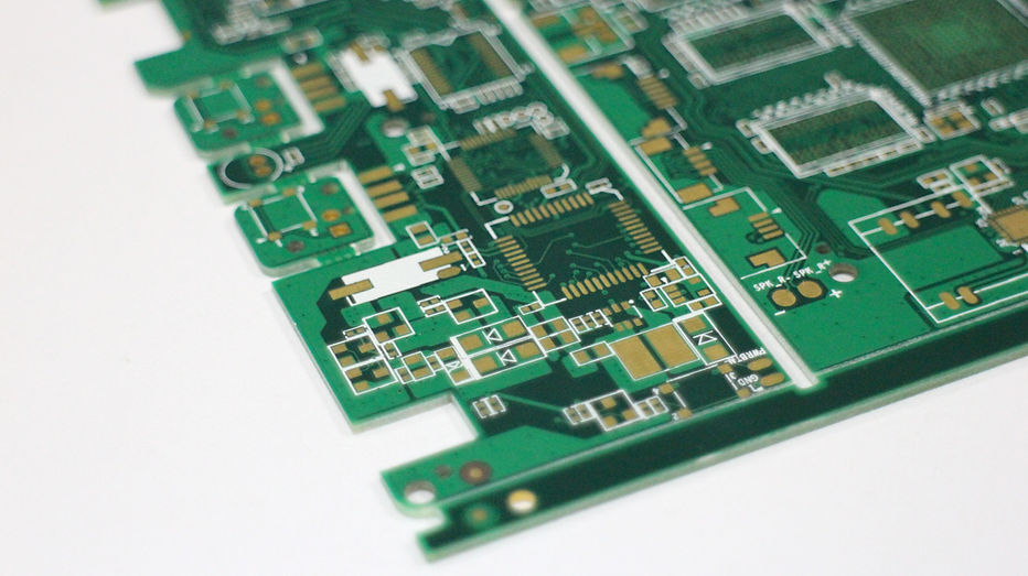
Both sides of Double-sided PCBs can be routed. It has components and conductive pathways on both sides of the board, which greatly reduces the difficulty of wiring, so it is widely used. Double-sided PCBs are more complex than single-sided boards and can provide more functionality in a smaller space. They are also more cost-effective than multi-layer PCBs, making them a popular choice for many electronic devices.
Besides, we also provide sampling and SMT service and customized high frequency high speed PCB.

Application:
Double-sided PCBs are used in a wide range of applications in the field of automotive electronics, telecommunications, industrial control, medical devices, consumer electronics, aerospace, computer, lighting, etc.
1. Automotive electronics:
Automotive electronics use double-sided PCBs to reduce weight, size, and cost. Examples include engine control modules, airbag systems, and anti-lock braking systems.
2. Telecommunications:
Double-sided PCBs are used in telecom applications such as base stations, routers, and switches.
3. Industrial Control:
Double-sided PCBs are used in industrial control applications such as PLCs, motion control systems, and robotics.
4. Medical Devices:
Double-sided PCBs are used in medical devices such as imaging systems, patient monitoring systems, and laboratory equipment.
5. Consumer Electronics:
Double-sided PCBs are used in consumer electronics such as mobile phones, digital cameras, and gaming consoles.
6. Military/Aerospace:
Double-sided PCBs are used in military and aerospace applications such as radar systems, guidance systems, and navigation systems.
7. Computer Peripherals:
Double-sided PCBs are used in computer peripherals such as hard drives, printers, and scanners.
8. Lighting:
Double-sided PCBs are used in lighting applications such as LED lighting, street lighting, and automotive lighting.

Customized Product:
One of our biggest advantage is the customized PCB. Customizing a double-sided printed circuit board (PCB) involves a number of steps:
1. Determine the desired board size and shape.
2. Choose a substrate material, such as FR-4, polyimide, or ceramic.
3. Design the board layout, including the placement of components, traces, and vias.
4. Create a bill of materials (BOM) listing all components to be used on the board.
5. Generate a fabrication drawing, which includes the board’s dimensions, layers, and other details.
6. Generate a Gerber file, which contains the design data for the board.
7. Submit the Gerber file and BOM to our factory for fabrication.
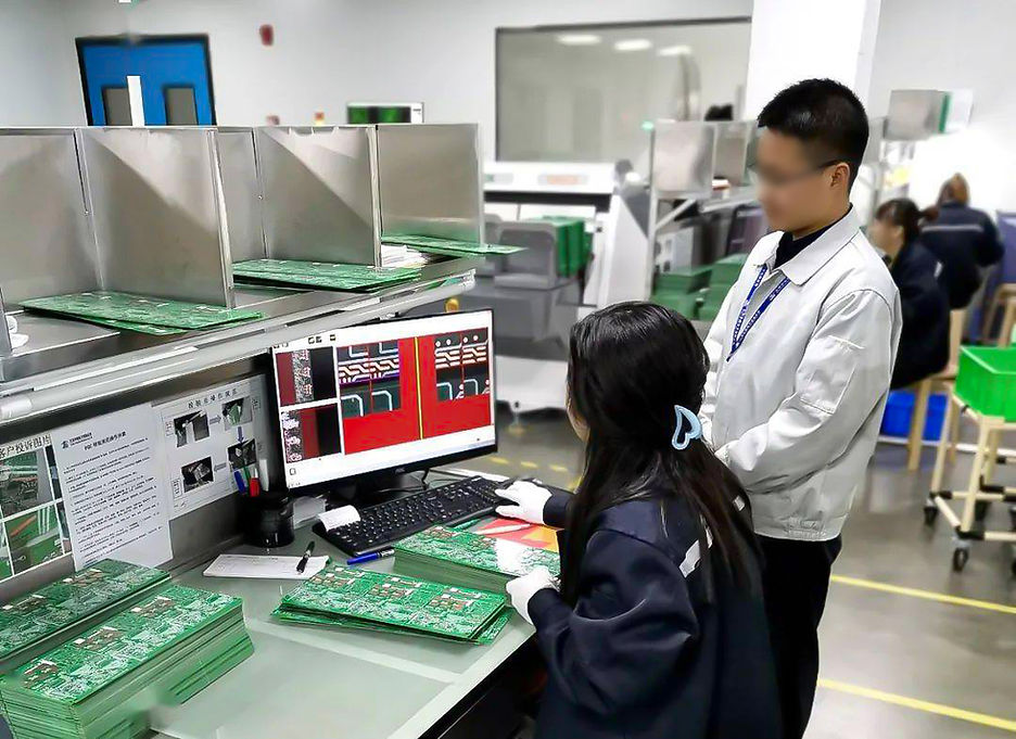
8. Inspect and test the boards to ensure they meet the customer’s requirements.
9. Package and ship the boards to the customer.

Production Features:
1. Long-term reliability management
Development from general automotive PCBs to heavy-duty PCBs.
2. Rich experience in the manufacturing technology of multi-layer PCBs
Full-range industrial control equipment and communication PCBs
3. Full range products, small-medium-large batches, short delivery time
・Small, medium and big QTY (1PC~2000㎡/Lot)
・Multiple varieties (3000~5000 product names/month)
4. Short lead times (for small batches)
5. Surface treatment: OSP, lead-free HASL (Sn-Ag-Cu, Sn-Ni-Cu), immersion gold, electro-gold, immersion tin
PCB Delivery Date:

Manufacturing Process:
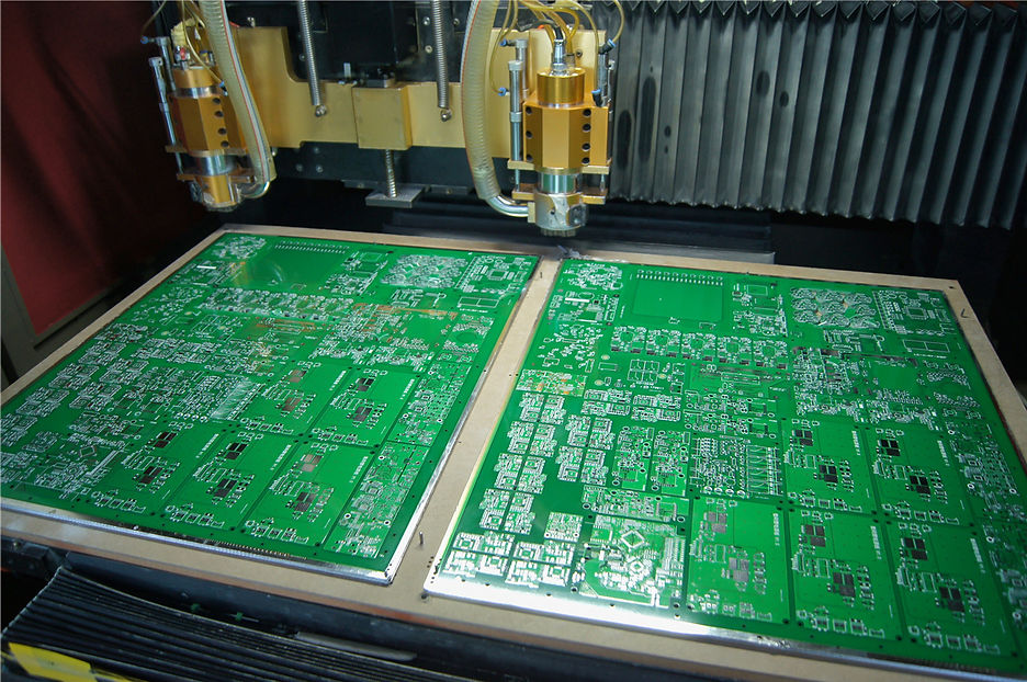
Copper clad plate cutting → Drilling → Copper plating → Outer layer graphic production → Resistance welding → Text → Surface treatment → Appearance processing → Electrical inspection → Appearance inspection → Packaging → Shipping.
